Nanotechnology is the design and manufacture of structures with at least one dimension between roughly 1 and 100 nanometres. It is defined by size rather than by material, because at that scale two things change: the proportion of atoms sitting on a surface becomes dominant, and quantum effects that are invisible in bulk start to set the material's colour, reactivity and strength.
- Nanotechnology is a claim about size, not substance. The same element behaves differently once its particles are small enough.
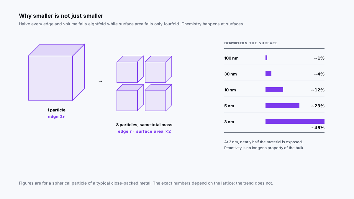
- Surface area is the first mechanism. About 1% of a 100 nm particle's atoms are on the surface; around 45% of a 3 nm particle's are.
- Quantum confinement is the second. Confine electrons within a few nanometres and their allowed energies separate into discrete steps.
- The 1–100 nm range is a convention with reasons. Below it you are doing chemistry; above it, bulk properties reassert themselves.
The number, and why the number is not the point
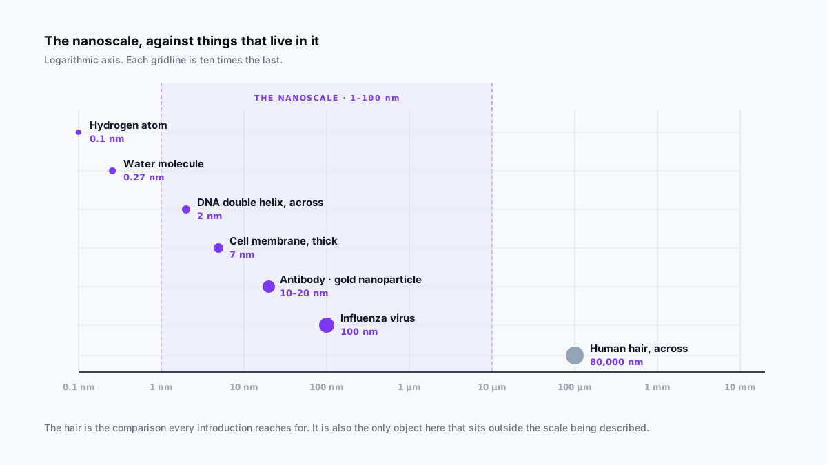
A nanometre is one billionth of a metre. Written out that is 0.000000001 m, and written out is exactly the problem: the digits are too far outside ordinary experience to carry meaning. Every introduction therefore reaches for a comparison, and almost all of them reach for the same one — a human hair, about 80,000 nm across.
That comparison fails in a specific way. It establishes that a nanometre is small relative to something visible, which the reader already assumed. It gives no sense of where a nanometre sits relative to the things that actually operate at that scale.
Better anchors are the ones at the same order of magnitude. A water molecule is 0.27 nm across. DNA is 2 nm wide. A cell membrane is 7 nm thick. An antibody is about 10 nm, and an influenza virus about 100. The nanoscale is not merely "very small" — it is the scale at which biological machinery is built, which is a large part of why it is worth engineering in.
Mechanism one: surfaces take over
Take a cube of material and halve every edge. Volume falls by a factor of eight; surface area falls by only four. Repeat this and the fraction of atoms exposed on the surface climbs from negligible to dominant.
For a typical metal, roughly 1% of the atoms in a 100 nm particle sit on its surface. At 10 nm it is around 12%. At 3 nm, close to half the material is exposed.
Since chemistry happens at surfaces, this changes a material's reactivity by orders of magnitude with no change to its composition. It is also why surface-to-volume ratio is the first thing to reach for when a nanoscale result seems surprising: often it is not surprising at all once you notice how much of the sample is surface.
The cleanest demonstration is gold. Bulk gold is yellow and famously unreactive — the reason it survives in jewellery for millennia. Gold reduced to 20 nm particles suspends in water as a deep red colloid and catalyses carbon monoxide oxidation at room temperature. Same element, same purity. Only the scale differs. Faraday made such a suspension in 1857; the original sample is still red and still at the Royal Institution.
Mechanism two: quantum effects stop averaging out
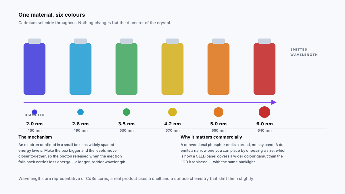
The second mechanism is not geometric. Confine an electron within a few nanometres and its permitted energy levels separate into discrete steps, in the way a particle in a small box has widely spaced states and one in a large box has closely spaced ones.
In a quantum dot this has a directly visible consequence: the emitted colour is set by the crystal's diameter rather than its chemistry. A 2 nm cadmium selenide dot fluoresces blue; a 6 nm dot of identical composition fluoresces red. You tune the optical property by changing a size, which is not something bulk materials allow.
Not every nanomaterial shows quantum confinement — it needs the right electronic structure and typically diameters below about 10 nm — but where it appears it is unambiguous evidence that you have left bulk behaviour behind.
Why 1 to 100 nanometres
National programmes and the research literature converge on this range, and the boundaries are conventions with reasons behind them rather than physical constants.
Below roughly 1 nm you are describing individual molecules, and the established vocabulary of chemistry describes them better. Above about 100 nm the surface fraction has dropped far enough, and confinement effects weakened enough, that most materials behave essentially as bulk.
Which is why "nanotechnology" is a claim about a size regime rather than about any particular material — and why a nanoparticle of an entirely familiar substance can be, functionally, a new one.
Two ways to build at this scale
Everything made at the nanoscale is made by one of two strategies, or by combining them.
Top-down
Top-down fabrication carves structures out of a larger block: lithography, etching, milling. This is how every processor chip is made. It is precise and well controlled, and its resolution is bounded by the tools — which at the leading edge cost more than most national research budgets.
Bottom-up
Bottom-up fabrication lets atoms and molecules arrange themselves. Self-assembly is the central idea: design the components so that the structure you want is their lowest-energy arrangement, then let thermodynamics do the positioning. This is cheap and massively parallel — trillions of structures form at once — and it is hard to steer, because you are limited to shapes the chemistry will actually favour.
Biology has been doing bottom-up assembly for several billion years, which is why so much of the field borrows from it.
What the field is not
Two persistent misconceptions are worth clearing, because both make it harder to read the literature.
The first is molecular assemblers — machines that build arbitrary structures atom by atom. This was a prominent 1980s proposal, it generated a serious technical dispute, and it is not what the field became. Working nanotechnology is chemistry, materials science and fabrication engineering.
The second is that "nano" on a product implies novel physics. It frequently means the particles are merely finely ground, which is not the same thing at all. A material is a nanomaterial when its behaviour departs from the bulk because of its size. Ground fine and behaving exactly as it always did, it is just a powder.
Sources & further reading
- National Nanotechnology Initiative — What is Nanotechnology? The definition most national programmes use. Link →
- Roduner, E. — Size matters: why nanomaterials are different. Chem. Soc. Rev. 35, 583–592 (2006). Link →
- Faraday, M. — Experimental Relations of Gold (and Other Metals) to Light. Phil. Trans. R. Soc. 147 (1857). Link →
- Whitesides, G. M. & Grzybowski, B. — Self-Assembly at All Scales. Science 295, 2418–2421 (2002). Link →
Common questions
Is nanotechnology one field?
No, and that is the usual source of confusion. It is a size regime that chemists, physicists, materials scientists, biologists and electronic engineers all work in, using different methods and publishing in different journals.
Are nanoparticles dangerous?
Some are, in some forms, by some routes of exposure — and the size that makes them useful is also what lets them cross barriers larger particles do not. It is an active regulatory area and the honest summary is that toxicity is particle-specific and cannot be generalised.
Where is nanotechnology already in everyday use?
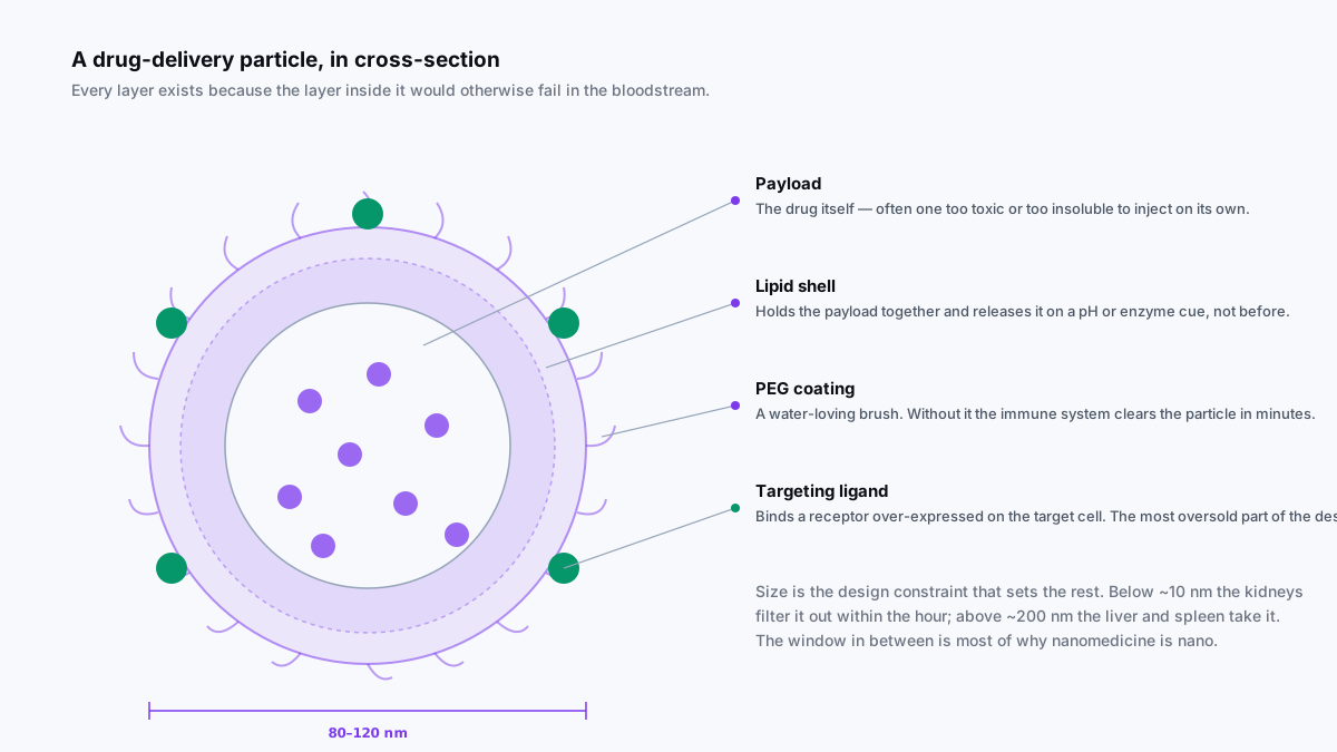
Sunscreens (zinc and titanium oxide particles), display panels (quantum dots), lithium battery electrodes, water filtration membranes, catalytic converters, and the lipid nanoparticles that delivered mRNA vaccines.
What background do I need to enter the field?
A physics, chemistry or materials degree is the usual route, with biology increasingly common for nanomedicine. The practical constraint is access: this is not a field you can practise without instrument time.