A quantum dot is a semiconductor nanocrystal small enough that its electrons' allowed energy levels are set by the crystal's physical size. A 2 nm cadmium selenide dot emits blue light and a 6 nm dot of identical composition emits red — so colour is tuned by controlling diameter, which is what makes them useful in displays.
- Colour is set by size, not chemistry. 2 nm emits blue, 6 nm emits red, with identical composition.
- The mechanism is quantum confinement. A smaller box means more widely spaced energy levels, so a higher-energy photon.
- The commercial advantage is a narrow emission band. A placeable, narrow peak beats a broad phosphor for colour gamut.
- The thirty-year delay was manufacturing. The physics was clear by 1984; controlling size distribution at scale was not.
A colour that depends on nothing but size
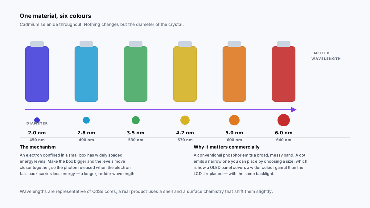
Prepare six vials of cadmium selenide nanocrystals differing only in diameter and illuminate them with ultraviolet light. The 2 nm sample fluoresces blue. The 6 nm sample fluoresces red. The four in between run through cyan, green, yellow and orange.
Same element. Same crystal structure. Same purity. The only variable is how big the crystals are.
This is the most direct demonstration available that nanoscale materials are not simply smaller versions of themselves, and it is why quantum dots appear in every introduction to the field.
The mechanism
In a bulk semiconductor, electrons occupy continuous bands of allowed energy. Excite one across the gap between bands and it eventually falls back, releasing a photon whose energy equals the gap. The gap is a property of the material, so the colour is fixed.
Shrink the crystal to a few nanometres and this stops being true. The electron is now confined in a space comparable to its own quantum-mechanical wavelength, and confinement forces its permitted energies apart — the standard particle-in-a-box result, where a smaller box has more widely spaced states.
The effective gap therefore widens as the crystal shrinks. A wider gap means a higher-energy photon, which means a shorter wavelength, which means bluer light. Quantum confinement in one sentence: smaller box, bigger gap, bluer light.
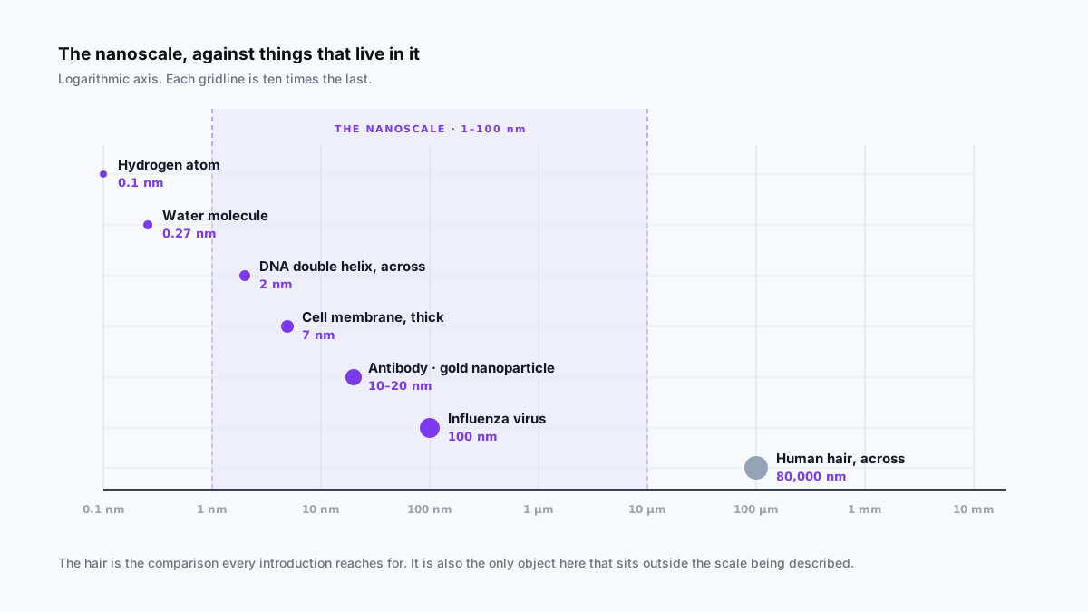
The effect switches on when the crystal is comparable to the material's exciton Bohr radius — a few nanometres for most semiconductors — which is exactly why quantum dots are nanoscale objects and not merely small ones.
Why a display manufacturer cares
The tunability is the demonstration. The commercial property is the shape of the emission peak.
A conventional phosphor emits a broad band — it produces "red" light spread across a wide range of wavelengths, much of which the display's colour filters then discard. A well-made quantum dot ensemble emits a narrow peak, and you place that peak wherever you want it by choosing a size.
The consequence is a wider colour gamut from the same backlight. A QLED panel is an LCD in which a blue LED backlight passes through a film of red- and green-emitting dots; the dots convert part of the blue into precisely the red and green the filters want. More of the light generated ends up as light you see, and the primaries are purer.
That is the entire commercial proposition, and it was enough to move quantum dots into mass production.
The thirty-year gap
Size-dependent emission in semiconductor nanocrystals was observed by Ekimov in glass in 1981 and by Brus in solution in 1983. The theory was settled within a few years.
Commercial displays shipped in 2013. The delay had almost nothing to do with physics.
Size distribution
If colour depends on diameter, then a sample with a broad distribution emits a broad, muddy band — the very problem quantum dots were supposed to solve. Useful material needs a standard deviation of a few percent, which meant developing synthesis routes with tight control over nucleation and growth. Hot-injection methods in the 1990s were the turning point.
Surface states
An early quantum dot was a poor emitter: much of the absorbed energy was lost at surface defects rather than emitted as light. The fix was a shell — a second semiconductor grown epitaxially over the core to passivate the surface. Core-shell architectures raised quantum yield from a few percent to near unity and are why modern dots are bright enough to be worth using.
Stability, and then scale
A dot that degrades under a backlight for eight hours a day for ten years is not a product, which meant further shells and barrier coatings. And all of it then had to work by the kilogram, which is a wholly separate discipline from making a good sample once.
What the timeline teaches
The thirty years were spent on size distribution, surface chemistry, stability and scale-up — every one of them a manufacturing problem rather than a scientific one.
This is the ordinary shape of nanotechnology reaching a product, and it is why the field's press coverage so consistently overshoots. A striking laboratory demonstration says the physics is real. It says very little about whether anyone can make a tonne of it with a 3% size distribution at a price a manufacturer will pay.
Cadmium is the current open question. It is toxic and restricted in consumer electronics in several jurisdictions, so a great deal of work has gone into cadmium-free alternatives — indium phosphide chiefly. They are in production and they are not yet as good, which is the field's most active quantum dot problem and a reminder that regulation is a design input rather than an afterthought.
Sources & further reading
- Murray, C. B., Norris, D. J. & Bawendi, M. G. — Synthesis and characterization of nearly monodisperse CdE semiconductor nanocrystallites. JACS 115, 8706–8715 (1993). Link →
- Brus, L. E. — Electron–electron and electron-hole interactions in small semiconductor crystallites. J. Chem. Phys. 80, 4403 (1984). Link →
- Nobel Prize in Chemistry 2023 — Scientific background on the discovery and synthesis of quantum dots. Link →
Common questions
Are quantum dots only used in displays?
No. They are widely used as fluorescent labels in biological imaging, where their brightness and photostability beat organic dyes, and are under active investigation for solar cells and photodetectors.
Is the cadmium in a QLED television dangerous?
The quantity is small and encapsulated, and several jurisdictions permit it under exemptions with concentration limits. The concern is manufacturing and end-of-life disposal rather than the panel in use — which is why cadmium-free alternatives are pursued so hard.
What is the difference between QLED and OLED?
QLED is an LCD whose backlight is colour-converted by quantum dots. OLED emits light from the pixel itself with no backlight, which is why it achieves true black. They are different display technologies, not variants of one.