
About Workshop
Discover how III-V semiconductor nanowires are reshaping the landscape of optoelectronics and photovoltaics. This mentor-guided workshop provides a comprehensive understanding of Vapor–Liquid–Solid (VLS) nanowire growth, nanowire-based lasing, and high-efficiency solar cell design.
Participants will explore how nanoscale geometry, band structure, and quantum confinement enable tunable optical and electronic properties. Through real-world case studies, they will learn how nanowire lasers and solar cells achieve superior performance through light confinement, heterostructure engineering, and efficient carrier transport.
Designed for students, researchers, and engineers in nanotechnology, materials science, and optoelectronics, this program bridges fundamental principles with device-level innovations driving next-generation photonic and energy technologies.
Structure
Day 1 – III-V Nanowire Basics & VLS Growth
- Introduction to III-V semiconductors (GaAs, InP, GaN, etc.)
- Nanowire geometry and quantum confinement effects
- Vapor–Liquid–Solid (VLS) growth mechanism
- Catalyst selection, supersaturation, and growth direction control
- Diameter, length, and crystal phase tuning (ZB vs WZ)
Day 2 – Optical Properties & Nanowire Lasers
- Optical modes, resonances, and waveguiding in nanowires
- Gain, feedback, and threshold behavior in nanowire lasers
- Core–shell and axial heterostructures for lasing
- Examples of room-temperature nanowire lasers
- Integration with photonic and on-chip optical systems
Day 3 – Nanowire Solar Cells & Photovoltaics
- Light absorption and trapping in nanowire arrays
- Axial and radial p–n junction architectures
- Surface recombination and passivation strategies
- Device efficiency, limitations, and real-world performance
- Tandem and multi-junction nanowire-based solar technologies
Important Dates
Registration Ends
4 PM
Workshop Dates
2026-01-15
5:30
5:30
What You Will Gain
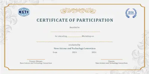
Outcomes
- Understand VLS growth dynamics and control parameters for III-V nanowires.
- Analyze quantum confinement and optical properties in nanoscale geometries.
- Design nanowire lasers with optimized gain and emission characteristics.
- Evaluate nanowire-based photovoltaic structures for enhanced light absorption.
- Gain insight into integration strategies for optoelectronic and energy devices.
Who Should Attend
- UG/PG students in Physics, Materials Science, Nanotechnology, or Electrical Engineering
- Researchers and academicians working on photonics, semiconductors, or solar cells
- Industry professionals focused on nanofabrication and advanced energy materials
- Enthusiasts seeking to understand nanowire device innovation and integration