| Attribute | Detail |
|---|---|
| Format | Online, self-paced course |
| Level | Basic / Beginner |
| Duration | 2–3 Weeks |
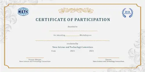
| Certification | e-Certification |
| Fee | ₹199 / $20 |
| Tools | Nanolithography Photolithography Electron Beam Lithography Nanoimprint Lithography Nanoscale Fabrication |
About the Basics of Nanolithography Course
The Basics of Nanolithography course is a free, beginner-friendly self-paced program designed to introduce learners to the techniques used to create extremely small patterns and structures at the nanoscale.
The course explains how nanolithography is used in semiconductor manufacturing, nanoelectronics, sensors, biomedical devices, and advanced materials research. Learners will explore basic concepts such as patterning, lithographic methods, nanoscale fabrication, and the role of nanolithography in modern technology.
Program Highlights
• Free beginner-level nanolithography course
• Online self-paced learning format
• Simple explanation of nanoscale patterning techniques
• Covers lithography methods, fabrication concepts, and nanoelectronics basics
• Real-world examples from semiconductor and nanotechnology industries
• Suitable for students and non-technical learners
• e-Certification upon successful completion
Course Curriculum
Module 1: Introduction to Nanolithography
- What is Nanolithography?
- Importance of Nanoscale Patterning
- Role of Nanolithography in Modern Technology
- Applications in Electronics and Nanotechnology
Module 2: Fundamentals of Lithography
- Basic Concepts of Pattern Transfer
- Masks, Substrates, and Resist Materials
- Resolution and Scaling Concepts
- Difference Between Micro- and Nanolithography
Module 3: Types of Nanolithography Techniques
- Photolithography Basics
- Electron Beam Lithography Concepts
- Nanoimprint Lithography Basics
- Scanning Probe and Soft Lithography Introduction
Module 4: Applications of Nanolithography
- Nanoelectronics and Semiconductor Devices
- Nanosensors and Biomedical Applications
- Nanophotonics and Optical Devices
- Advanced Materials and Surface Engineering
Module 5: Future Scope and Learning Path
- Emerging Trends in Nanolithography
- Challenges in Nanoscale Manufacturing
- Career Opportunities in Nanotechnology and Semiconductor Engineering
- Mini Learning Activity / Concept-Based Practice
Tools, Techniques, or Platforms Covered
Nanolithography Photolithography Electron Beam Lithography Nanoimprint Lithography Nanoscale Fabrication
Real-World Applications
- Developing nanoscale semiconductor devices
- Creating advanced nanoelectronic circuits
- Supporting biomedical sensor fabrication
- Improving nanoscale optical and photonic devices
- Preparing for advanced learning in nanotechnology and semiconductor manufacturing
Who Should Attend & Prerequisites
- This course is suitable for students, beginners, engineering learners, electronics learners, nanotechnology learners, and professionals interested in nanoscale fabrication technologies.
- It is also useful for learners from nanotechnology, semiconductor engineering, electronics, materials science, physics, chemistry, and advanced manufacturing backgrounds.
Certification